MC14093 (CMOS) Quad 2-Input NAND Schmitt TriggerData sheetDirect Replacement for CD4093, MC14011Bby Tony van Roon
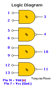
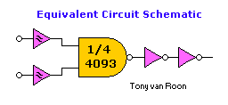
The MC14093B Schmitt Trigger is constructed with MOS P-channel and N-channel enhancement mode devices in a single monolithic structure. These devices find primary use where low power dissipation and/or high noise immunity is desired. The MC14093B may be used in place of the MC14011B quad 2-input NAND gate for enhanced noise immunity or to "square-up" slowly changing waveforms.
Features:
Supply voltage range is 3.0Vdc to 18Vdc.
Capable of driving two low-power TTL loads or one low-power Schottky TTL load over the rated temperature range.
Double diode protection on ALL inputs.
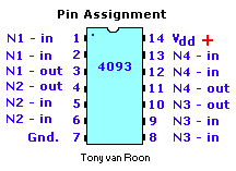
Pin-for-pin compatible with the CD4093.
Can be used to replace the MC14011B.
Absolute Maximum Ratings:
Supply voltage for MC14093B is -0.5 to +18 volt dc.
Input or Output voltage (DC or Transient) -0.5 to Vdd +0.5volt dc.
Input or Output current (DC or Transient), per pin is approx. 10mA.
Power dissipation 500 milliWatts.
Storage temperature range from -65 to +150 °C.
Lead temperature (soldering, up to 8 sec) 260 °C.
Suffix's:
The 'L' suffix stands for Ceramic package (mostly used in the Industry), case 632.
The 'P' suffix stands for Plastic package, case 646.
Notes:
- Tie unused inputs always to an appropriate voltage level like +Vcc or Ground. Unused outputs must remain open.
- The MC14093B contains protection circuitry to guard against damage due to high static voltages or electric field. However, precautions must be take to avoid applications of any voltage higher than maximum rated voltage to this high impedance circuit. For proper operation, Vin and Vout should be constrained to the range Vss smaller-than Vdd.

