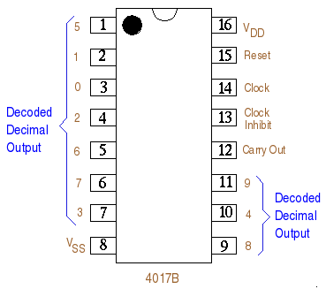
CP0 (clock pulse zero) is the Clock input, Pin 14 on the diagram above.
CP1 (clock pulse one) is the clock inhibit or Pin 13 on the pinout above.
MR (master reset) is the reset pin 15 in the diagram above.
Q0-9 represent the decoded decimal outputs. Hence Q0 is Pin 3 on the pinout and Q8 is Pin9.